Page 1 of 1

IBM introduces 2 nm node chip

Posted: Fri May 07, 2021 6:43 am
by shpalman
IBM Introduces the World’s First 2-nm Node Chip

Image

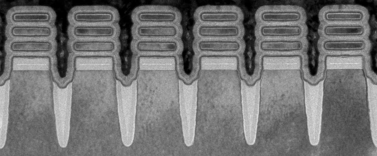
Well if I were the referee I'd point out there's no scale bar on that. But this helps explain what we're looking at:

Image

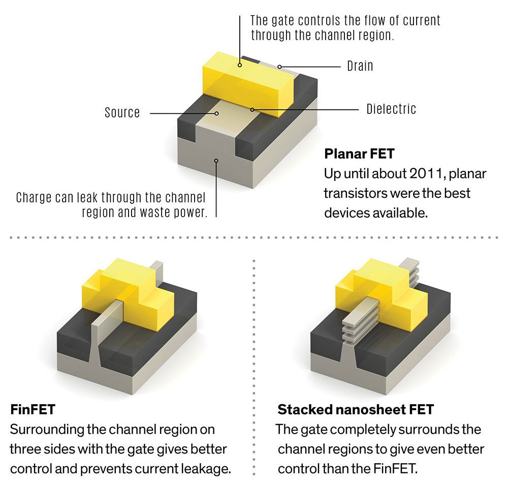
(from The Nanosheet Transistor Is the Next (and Maybe Last) Step in Moore’s Law)

I noted that the process uses silicon germanium, but only because there are chemicals which etch SiGe and not Si, so you can etch the SiGe layers away from between the Si to leave these free-standing Si ribbons.

Re: IBM introduces 2 nm node chip

Posted: Fri May 07, 2021 7:54 am
by jaap
Regarding the scale, I read that the "2nm" is no longer a real size measure but a kind of proxy equivalent. The transistors are now stacked up in several layers, but if you were able to squeeze them all in a single layer, then you would need a 2nm resolution to make it. The resolution used to produce these chips is actually less than that, but it is damned impressive nevertheless.

Re: IBM introduces 2 nm node chip

Posted: Fri May 07, 2021 4:30 pm
by basementer
There's something analogous going on in the time domain. The speculative instruction execution of current processors is so accurate that a fixed point add operation takes, on average, less than one clock cycle. (Mentioned in one of Lex Fridman's YouTube interviews, I'll try to find the source tomorrow.)

Re: IBM introduces 2 nm node chip

Posted: Sat May 08, 2021 12:47 am
by basementer
basementer wrote:
Fri May 07, 2021 4:30 pm
There's something analogous going on in the time domain. The speculative instruction execution of current processors is so accurate that a fixed point add operation takes, on average, less than one clock cycle. (Mentioned in one of Lex Fridman's YouTube interviews, I'll try to find the source tomorrow.)
it was in this conversation with Jim Keller:
https://www.youtube.com/watch?v=Nb2tebYAaOA